Difference between revisions of "Examples and reference designs"
| Line 1: | Line 1: | ||
| − | The next examples present typical cases of using the Evariste II system. They include both simulation and synthesis projects and script files for testbenches and hardware testing. The first project has five different versions – one version for each available FPGA device (module). The second project is built only for Altera Cyclone III device, but it can be adapted very easily to any of available devices (only PLL configuration and device pinout need to be changed). | + | The next examples present typical cases of using the Evariste II system. They include both simulation and synthesis projects and script |
| + | |||
| + | files for testbenches and hardware testing. The first project has five different versions – one version for each available FPGA device | ||
| + | |||
| + | (module). The second project is built only for Altera Cyclone III device, but it can be adapted very easily to any of available devices | ||
| + | |||
| + | (only PLL configuration and device pinout need to be changed). | ||
=High speed data transfer from the FPGA module via USB= | =High speed data transfer from the FPGA module via USB= | ||
| − | This project demonstrates the way how high speed one directional data transfers can be made. It also shows what data rate can be obtained in full-speed hardware tests. It implements a simple bi-directional counter accessible from the USB bus. | + | This project demonstrates the way how high speed one directional data transfers can be made. It also shows what data rate can be obtained |
| + | |||
| + | in full-speed hardware tests. It implements a simple bi-directional counter accessible from the USB bus. | ||
==Hardware design== | ==Hardware design== | ||
| − | The hardware design is composed of 8 vhdl files placed in the ''shared'' folder (folder ''synth'' does not contain any files in this | + | The hardware design is composed of 8 vhdl files placed in the ''shared'' folder (folder ''synth'' does not contain any files in this |
| + | example). The list of user files in project folder(s) is presented in the next table (in alphabetical order): | ||
| − | |||
| − | + | [[Image:Synthtransfer2usb.jpg]] | |
| − | Implementation of the transfer2usb project in different FPGA families does not need any design constraints. In order to obtain maximum speed, we recommend to set the ''clk_ctrl'' clock as close to 48 MHz as possible (maximum frequency allowed by Cypress). | + | The application module implements two modes (which are determined using bits ''ctrl2appl(2 .. 0)'' of the control register implemented in |
| + | |||
| + | the top level entity transfer2usb): MODE_TST0 and MODE_TST1. In mode MODE_TST0 (''ctrl2appl(2 .. 0)'' = “011”), a 128-bit counter is | ||
| + | |||
| + | incremented after each data request. In MODE_TST1 (''ctrl2appl(2 .. 0)'' = “111”), the same counter is decremented. The counter is | ||
| + | |||
| + | implemented in the ''applic_wrp.vhd'' file. Mode names and values are defined in the ''lab_hc_pkg.vhd'' file. The same values must be used | ||
| + | |||
| + | in the software (script) calling the hardware. | ||
| + | |||
| + | Implementation of the transfer2usb project in different FPGA families does not need any design constraints. In order to obtain maximum | ||
| + | |||
| + | speed, we recommend to set the ''clk_ctrl'' clock as close to 48 MHz as possible (maximum frequency allowed by Cypress). | ||
==VHDL simulation using scripts== | ==VHDL simulation using scripts== | ||
| − | The ModelSim project is placed in the simul directory. After launching the ModelSim software, the user should first change the directory (File -> Change Directory...). Then he should write in the Transcript window: ''do tb.do'' in order to launch compilation and simulation. The simulator will open the ''bus_script_in.txt'' text file containing the script; it will then read commands and data and stimulate DUT. Generated waveforms will be displayed in the Waveform window and the response of the DUT will be written to the log file. The next table shows the structure of user files using in simulation. | + | The ModelSim project is placed in the simul directory. After launching the ModelSim software, the user should first change the directory |
| + | |||
| + | (File -> Change Directory...). Then he should write in the Transcript window: ''do tb.do'' in order to launch compilation and simulation. | ||
| + | |||
| + | The simulator will open the ''bus_script_in.txt'' text file containing the script; it will then read commands and data and stimulate DUT. | ||
| + | |||
| + | Generated waveforms will be displayed in the Waveform window and the response of the DUT will be written to the log file. The next table | ||
| + | |||
| + | shows the structure of user files using in simulation. | ||
| + | |||
| + | |||
| + | [[Image:Simultransfer2usb.jpg]] | ||
| + | |||
| + | |||
| + | The next figure shows input script file | ||
| + | |||
| + | |||
| + | [[Image:Ex1_scriptin.jpg]] | ||
| + | |||
| + | |||
| + | The next figure shows output log file contents (as a response to the input script file) | ||
| + | |||
| + | |||
| + | [[Image:Ex1_logout.jpg]] | ||
Latest revision as of 03:40, 8 April 2013
The next examples present typical cases of using the Evariste II system. They include both simulation and synthesis projects and script
files for testbenches and hardware testing. The first project has five different versions – one version for each available FPGA device
(module). The second project is built only for Altera Cyclone III device, but it can be adapted very easily to any of available devices
(only PLL configuration and device pinout need to be changed).
High speed data transfer from the FPGA module via USB
This project demonstrates the way how high speed one directional data transfers can be made. It also shows what data rate can be obtained
in full-speed hardware tests. It implements a simple bi-directional counter accessible from the USB bus.
Hardware design
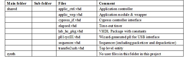
The hardware design is composed of 8 vhdl files placed in the shared folder (folder synth does not contain any files in this
example). The list of user files in project folder(s) is presented in the next table (in alphabetical order):
The application module implements two modes (which are determined using bits ctrl2appl(2 .. 0) of the control register implemented in
the top level entity transfer2usb): MODE_TST0 and MODE_TST1. In mode MODE_TST0 (ctrl2appl(2 .. 0) = “011”), a 128-bit counter is
incremented after each data request. In MODE_TST1 (ctrl2appl(2 .. 0) = “111”), the same counter is decremented. The counter is
implemented in the applic_wrp.vhd file. Mode names and values are defined in the lab_hc_pkg.vhd file. The same values must be used
in the software (script) calling the hardware.
Implementation of the transfer2usb project in different FPGA families does not need any design constraints. In order to obtain maximum
speed, we recommend to set the clk_ctrl clock as close to 48 MHz as possible (maximum frequency allowed by Cypress).
VHDL simulation using scripts
The ModelSim project is placed in the simul directory. After launching the ModelSim software, the user should first change the directory
(File -> Change Directory...). Then he should write in the Transcript window: do tb.do in order to launch compilation and simulation.
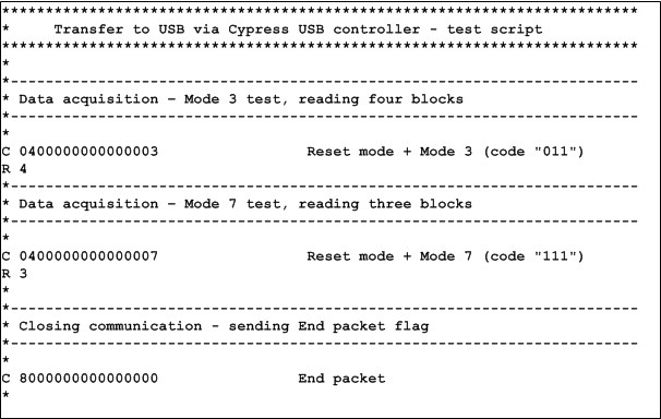
The simulator will open the bus_script_in.txt text file containing the script; it will then read commands and data and stimulate DUT.
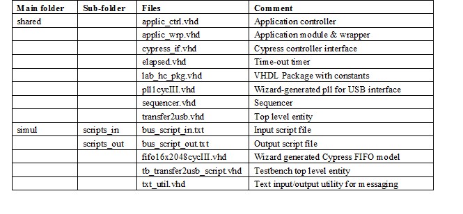
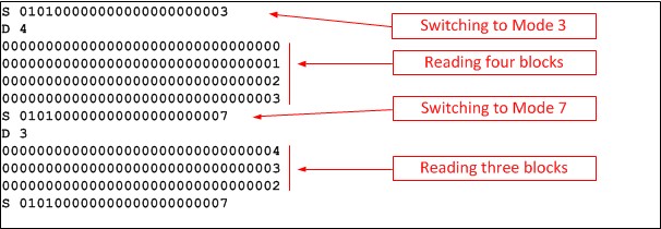
Generated waveforms will be displayed in the Waveform window and the response of the DUT will be written to the log file. The next table
shows the structure of user files using in simulation.
The next figure shows input script file
The next figure shows output log file contents (as a response to the input script file)


