Difference between revisions of "Hardware"
| Line 10: | Line 10: | ||
| − | [[Image: | + | [[Image:Hardware.jpg]] |
| Line 35: | Line 35: | ||
===Low cost Altera Cyclone III module, version 2.2=== | ===Low cost Altera Cyclone III module, version 2.2=== | ||
| − | [[Image: | + | [[Image:CycloneIIIv22_sm.jpg]] |
The low cost Altera module v. 2.2 features: | The low cost Altera module v. 2.2 features: | ||
| Line 47: | Line 47: | ||
===Low cost Altera Cyclone III module, version 2.4=== | ===Low cost Altera Cyclone III module, version 2.4=== | ||
| − | [[Image: | + | [[Image:CycloneIIIv24_sm.jpg]] |
The second available version of the low cost Altera module (v. 2.4) features: | The second available version of the low cost Altera module (v. 2.4) features: | ||
| Line 59: | Line 59: | ||
==FPGA module with a high performance Altera family== | ==FPGA module with a high performance Altera family== | ||
| − | [[Image: | + | [[Image:ArriaIIv10_sm.jpg]] |
The high end Altera module features: | The high end Altera module features: | ||
| Line 71: | Line 71: | ||
==FPGA module with a low cost Xilinx family== | ==FPGA module with a low cost Xilinx family== | ||
| − | [[Image: | + | [[Image:Spartan3v21_sm.jpg]] |
The low cost Xilinx module v. 2.1 features: | The low cost Xilinx module v. 2.1 features: | ||
| Line 83: | Line 83: | ||
==FPGA module with a high performance Xilinx family== | ==FPGA module with a high performance Xilinx family== | ||
| − | [[Image: | + | [[Image:Virtex5v10b_sm.jpg]] |
The high end Xilinx module v 1.0b features: | The high end Xilinx module v 1.0b features: | ||
| Line 95: | Line 95: | ||
==FPGA module with a non volatile Microsemi technology== | ==FPGA module with a non volatile Microsemi technology== | ||
| − | [[Image: | + | [[Image:Fusionv20_sm.jpg]] |
The Microsemi module v. 2.0 features: | The Microsemi module v. 2.0 features: | ||
Revision as of 01:36, 8 April 2013
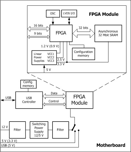
The hardware consists of a motherboard and six types of application modules. All application modules are built around an FPGA device from one of five selected FPGA families: Altera Cyclone III and Arria II, Xilinx Spartan 3 and Virtex 5 and Microsemi Fusion. All the modules have the same architecture and topology in order to guarantee a fair comparison of hardware dependent cryptographic functions implemented in different FPGA technologies. Each module contains (see figure below):
- Selected FPGA device
- Configuration memory (only modules with SRAM technology FPGAs)
- Low noise linear power supply regulators
- 4MB SRAM memory with a 32-bit data access
- 16 MHz quartz oscillator
- Data interface connectors including several LVDS (Low Voltage Differential Signaling) signals
All modules contain a proprietary configuration interface and FPGA vendor defined configuration connectors. The modules are plugged into the motherboard, which contains the USB interface hardware controller and power supplies.
Contents
Motherboard
The motherboard features the Cypress EZ USB device CY 7C68013A – 100 ACX and its configuration memory (accessible by the original Cypress software), linear power supplies and high quality low pass ferrite filters. All kinds of available FPGA modules can be plugged into the motherboard (the high end Xilinx module needs the motherboard to be slightly modified). Besides the USB interface controllers, the motherboard contains linear power supplies, high quality low pass ferrite filters and necessary connectors. The motherboard can be supplied from a 12 V battery, 5 V external power supply or the USB bus. It delivers a 5 V power supply (3.3 V for the Xilinx Virtex 5) to the FPGA module.
FPGA modules
Six hardware modules having the same topology are available. They contain: one FPGA device, FPGA configuration interface and eventually configuration memory (for SRAM-based FPGAs), one 16 MHz quartz oscillator and at least two connectors for LVDS data interface. Most of modules contain also a 4 MB SRAM block (optional) with the 32-bit data interface.
FPGA modules with a low cost Altera family
Two versions of the low cost Altera module are available: the standard one (version 2.2) has the same structure as FPGA modules for other families (Xilinx and Microsemi) and the second one (version 2.4) is optimized for implementation of side-channel attacks. In this second version of the module, the SRAM memory block is omitted and some filters and connectors for the power trace acquisition are added.
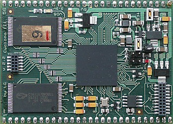
Low cost Altera Cyclone III module, version 2.2
The low cost Altera module v. 2.2 features:
- Altera Cyclone III EP3C25F256-C8 FPGA device
- 16-Mbit non volatile serial configuration memory EPCS16
- 16 MHz quartz oscillator
- Two low power 2MB asynchronous SRAM memories Cypress CY62167DV300LL with 2 x 16-bit data bus
- Linear power supply regulators giving 3.3 V (VCCIO), 2.5 V (for LVDS I/Os and analog part of PLLs) and 2 x 1.2 V (for VCCINT and digital part of PLLs)
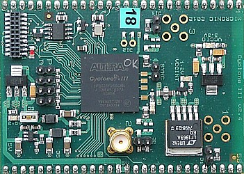
Low cost Altera Cyclone III module, version 2.4
The second available version of the low cost Altera module (v. 2.4) features:
- Altera Cyclone III EP3C25F256-C8 FPGA device
- 16-Mbit non volatile serial configuration memory EPCS16
- 16 MHz quartz oscillator
- Linear power supply regulators giving 3.3 V (VCCIO), 2.5 V (for LVDS I/Os and analog part of PLLs) and 2 x 1.2 V (for VCCINT and digital part of PLLs)
- Set of connectors aimed at implementation of side channel attacks (easy plug-in of differential probes, inclusion of serial resistors, etc.)
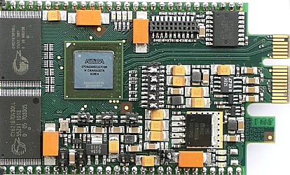
FPGA module with a high performance Altera family
The high end Altera module features:
- Altera Arria II GX EP2AGX45CU17C6 FPGA device
- 16-Mbit non volatile serial configuration memory EPCS16
- 16 MHz quartz oscillator
- Two low power 2MB asynchronous SRAM memories Cypress CY62167DV300LL with 2 x 16-bit data bus
- Linear power supply regulators giving 3.3 V (VCCIO), 2 x 2.5 V (for LVDS and analog parts of PLLs), 1.5 V together with 1.1 V (for transceiver) and 0.9 V (for VCCINT and for digital parts of PLLs).
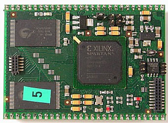
FPGA module with a low cost Xilinx family
The low cost Xilinx module v. 2.1 features:
- Xilinx Spartan 3 XC3S700AN-FFG484 device
- 16 MHz quartz oscillator
- FLASH configuration memory AT45DB161D
- Two low power 2MB asynchronous SRAM memories Cypress CY62167DV300LL with 2 x 16-bit data bus
- Linear power supply regulators giving 3.3 V (VCCIO) and 1.2 V (for VCCINT).
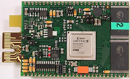
FPGA module with a high performance Xilinx family
The high end Xilinx module v 1.0b features:
- Xilinx Virtex 5 XC5VLX30T-FFG323 device
- 16-Mbit non volatile FLASH configuration memory AT45DB161D
- 25 MHz quartz oscillator
- Two low power 2MB asynchronous SRAM memories Cypress CY62167DV300LL with 2 x 16-bit data bus
- Linear power supply regulators giving 3.3 V (VCCIO), 3 x 2.5 V (for LVDS I/Os, system monitor and auxiliary circuitry) and 2 x 1.2 V (RocketIO GTP transceivers) and 2 x 1.0 V (VCCINT and RocketIO GTP transceivers)
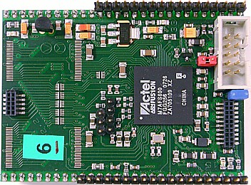
FPGA module with a non volatile Microsemi technology
The Microsemi module v. 2.0 features:
- Microsemi Fusion M7AFS600 FGG256X2 device
- 16 MHz quartz oscillator
- Two low power 2MB asynchronous SRAM memories Cypress CY62167DV300LL with 2 x 16-bit data bus
- Linear power supply regulators giving 3.3 V (VCCIO, VCCOSC, VCCA, VJTAG and VPUMP) and 2.6 V (LVDS). The 1.5 V is controlled by the internal power supply regulator and an external transistor (the power supply pins VCCINT, VCCPLL and VCC15A).
