Introduction
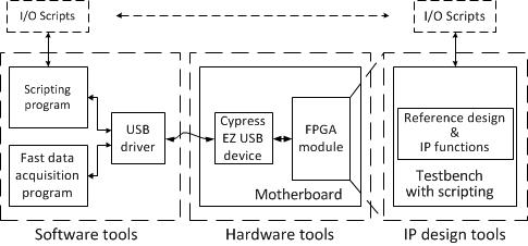
The system Evariste III is aimed at development and evaluation of cryptographic functions and primitives in reconfigurable hardware. It is an evolution of the Evariste II system. It consists of a set of hardware, software and design tools making the development and evaluation of cryptographic functions easier. All the tools are open source and their reliable function was approved in many projects.
The hardware part of the system is composed of a module that contains an FPGA device. The module is plugged into a motherboard that contains power supply and communication elements. The first version of the system (Evariste II) includes five modules, each containing one of selected FPGA devices:
- Altera Cyclone III (EP3C25)
- Altera Arria II (EP2AGX45)
- Xilinx Spartan 3 (XC3S700AN)
- Xilinx Virtex 5 (XC5VLX30T)
- Actel Fusion (M7AFS600)
Besides FPGA device, some modules contain a 4MB SRAM memory with a 32-bit data access. All the modules have identical pin-out and can be plugged into the motherboard containing the Cypress EZ USB controller device thanks to a 56 pins dip connector. In order to reduce the noise in the context of random number generation or side channel attacks, all the modules and motherboards use only linear voltage regulators as FPGA power supplies. The hardware can be accessed from the PC via USB bus using an open source signed GNU driver compatible with Windows XP and Windows 7 – 10.
The Evariste III system includes some improvements. The new motherboard (V1.2) contains ZIF (zero insertion force) connectors to easily plug and unplug modules in a safe way. It also includes a JTAG chain that enables to configure several FPGAs through the same JTAG bus (this is very helpful in PUF characterization that needs numerous data acquisitions to be performed in different operating conditions). Eight extra pins have been added to the module connector to dispatch these JTAG signals. All old modules are still compatible with the new motherboard, letting 8 pins free, but the new modules are not compatible anymore with the old, V1.1, motherboard.
Three types of application modules have been designed for this new modular system. Each module is built around different FPGA family:
- Xilinx Spartan 6 (XC6SLX16)
- Altera Cyclone V (5CEBA4F17C8N)
- Microsemi SmartFusion2 (M2S025-FG484)
The devices of the last family represent an embedded SoC based on an ARM processor. Besides the necessary hardware, the Evariste II/III system consist of a set of open source hardware design tools and an open source control and data acquisition software. The reconfigurable hardware design is made of four main IP (intellectual property) functions (USB controller interface, packet manager, application controller and application itself) and a testbench file for simulations.
The hardware part of the system uses one of five available modules containing one of selected FPGA devices:
- Altera Cyclone III (EP3C25)
- Altera Arria II (EP2AGX45)
- Xilinx Spartan 3 (XC3S700AN)
- Xilinx Virtex 5 (XC5VLX30T)
- Microsemi Fusion (M7AFS600)
Besides FPGA device, some modules contain a 4MB SRAM memory with a 32-bit access. All the modules have identical pin-out and can be plugged into the motherboard containing the Cypress EZ USB controller device. In order to reduce the noise in the context of random number generation or side channel attacks, all the modules and motherboards use only linear voltage regulators as FPGA power supplies. The hardware can be called via USB bus using approved original drive from Cypress.
The reconfigurable hardware design consist of four main parts – IP (intellectual property) functions:
- USB controller interface
- Packet manager
- Application controller
- Application itself
The USB controller interface and the packet manager shouldn’t be modified by the user (their proper operation was already approved in many circumstances). The used should just adapt the application controller to the application needs and he should design his own application IP (for example by using existing examples).
Both software and hardware interface design tools can take benefit from the use of an equivalent scripting environment using identical commands and syntax. Both the VHDL testbench and the software command interpreter (script.exe) can read the same script file and generate the log file using the same syntax. This makes development of the data interface hardware and software very easy, since the same script can be used in both VHDL testbenches and hardware tests using software calls of hardware functions.
Once the hardware functions and their software calls are designed, tested and approved using scripting language commands, the final high-speed software using identical calls of hardware functions can be easily developed. Since both scripting software and application software use the same MS Windows driver, the calls of hardware functions are always perfectly controlled. Several examples of constructing executable files are available.
The concept of the two scripting environments together with the design of efficient software calls guarantees high flexibility and fast design process, but also very fast data interface in the final software version. Depending on the character of communications (one or two directional), the throughput can attain 40 MB/s (bulk USB mode). When using the optional SRAM memory available on the modules, the sustainable data acquisition rate can be as high as 400 Mbits/s.
